Notes on Reflow of Chip Resistors
author: Milliohm Electronic
2025-09-12
I: Component Characteristic Matching
Package Size Matching: Different packages (such as 0402, 0805, and 1206) have significantly different process sensitivities.
Small packages (0201/0402): "Tombstone" (uneven solder tension on the pads at both ends) can easily occur due to variations in solder paste volume, requiring strict control of solder paste printing accuracy.
Large packages (1206 and above): Due to their large thermal capacity, sufficient temperature penetration during the reflow phase must be ensured to prevent cold solder joints. At the same time, attention should be paid to the stress impact of PCB thermal deformation on the solder joints.
II: Solder Paste Printing and Pad Design
① Solder Paste Parameter Optimization
Type Selection: Select a matching solder paste based on the resistor terminal material (mostly Sn/Pb or lead-free coating) (e.g., Sn-Ag-Cu solder paste for lead-free resistors, melting point 217°C) to prevent abnormal growth of intermetallic compounds.
Printing volume control: The solder paste volume must match the pad size. For small-package resistors, excessive solder paste can cause bridging, while insufficient solder paste can result in cold solder joints. The recommended stencil aperture should cover 80%-90% of the pad area, with a thickness of 0.1-0.15mm (adjusted depending on the package).
② Pad Design Specifications
The pad shape should be symmetrical (avoid one end being wider than the other), 0.2-0.3mm longer than the resistor body, and consistent in width (±0.1mm) with the resistor width to reduce the risk of "tombstone" soldering.
The pad spacing should match the spacing between the resistor's electrodes (tolerance ≤ 0.05mm). Excessive spacing can cause cold solder joints, while too little spacing can cause bridging.
The pad spacing should match the spacing between the resistor's electrodes (tolerance ≤ 0.05mm). Excessive spacing can cause cold solder joints, while too little spacing can cause bridging.
III: Reflow Oven Temperature Profile Adjustment
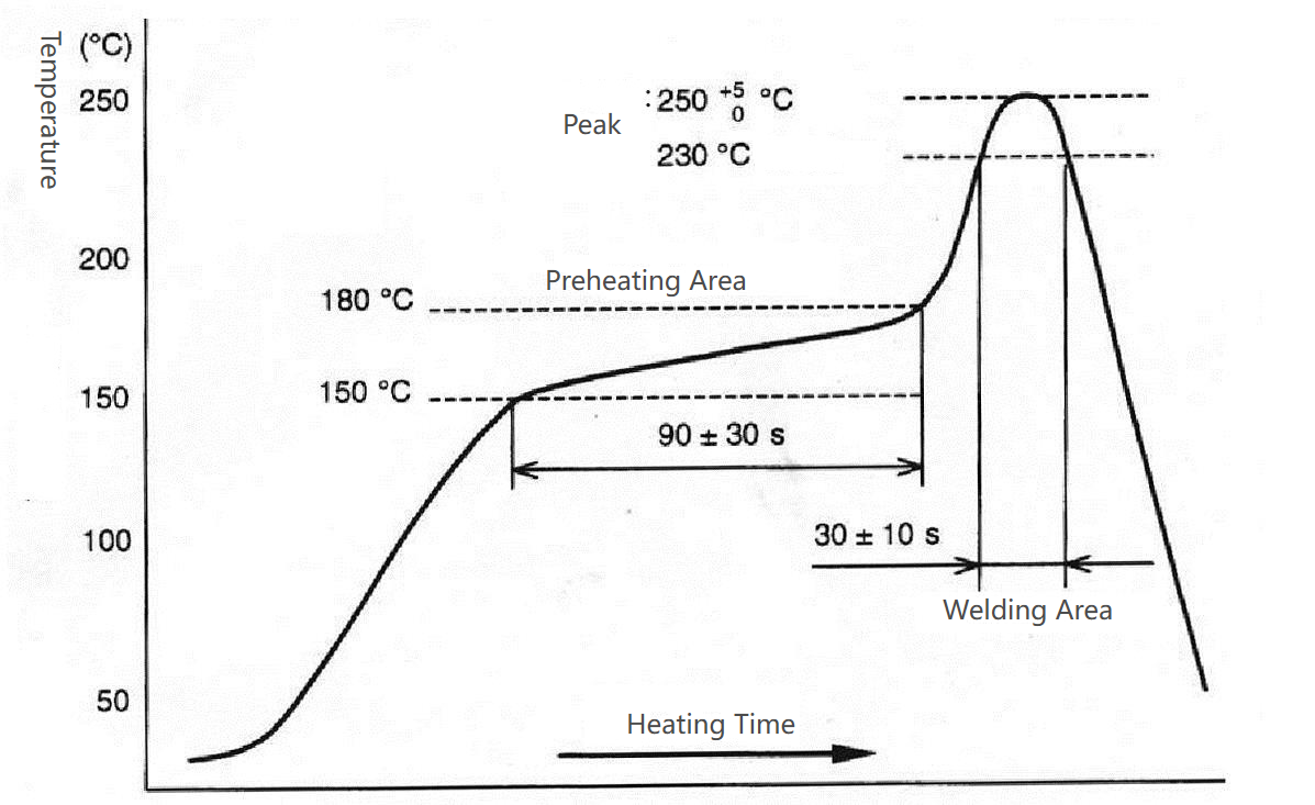
① Four-Stage Profile Control
Preheating Stage (80-150°C): Ramp rate ≤ 2°C/second to slowly evaporate the solvent in the solder paste to prevent spattering and solder beads. This stage should last 60-120 seconds to avoid thermal stress on the component due to rapid heating.
Constant Temperature Stage (150-180°C): Activates the flux and removes the oxide layer on the pads and electrodes for 60-90 seconds to prevent premature flux depletion and solder joint oxidation.
Reflow Stage (Peak Temperature 230-250°C, Lead-Free Process): Peak temperature is 20-30°C higher than the solder paste melting point to ensure complete solder melting; high temperature (>217°C) duration is controlled within 30-60 seconds to prevent resistor overheating.
Cooling Stage (from peak to 150°C): Cooling rate is 1-3°C/second. Rapid cooling ensures dense solder joint crystallization and reduces voids.
② Ensuring Temperature Uniformity
The PCB surface temperature difference must be ≤±5°C. Avoid localized overheating around large copper sheets and heat sinks, or insufficient temperature at the edges (unmelted solder). The furnace air flow can be optimized by increasing temperature measurement points (e.g., attaching thermocouples near dense resistor areas).
IV: Solder Defect Prevention and Detection
① Common Defects and Countermeasures
Tombstone: Check pad symmetry, adjust solder paste printing volume (evenly distributed on both ends), and reduce preheating temperature.
Bridging: Reduce stencil aperture size, optimize printing pressure (to prevent solder paste collapse), and increase pad spacing.
Hot Solder Joints/Voids: Ensure pads are free of oxidation (OSP or immersion gold treatment can be used), and control reflow peak temperature and time to prevent premature flux evaporation.
② Quality Inspection
After soldering, inspect solder joints using AOI (Automated Optical Inspection) for appearance (fullness and burr-free). For critical circuits, use X-ray to check for void content within solder joints (must be ≤20%). Re-measure resistor values to confirm there is no drift due to high temperatures.
Note: For further information on products, solutions, or specific application scenarios, please feel free to contact technical support.
Derating principles for alloy resistors
The impact of parasitic inductance on circuits in resistor applications
Related Article
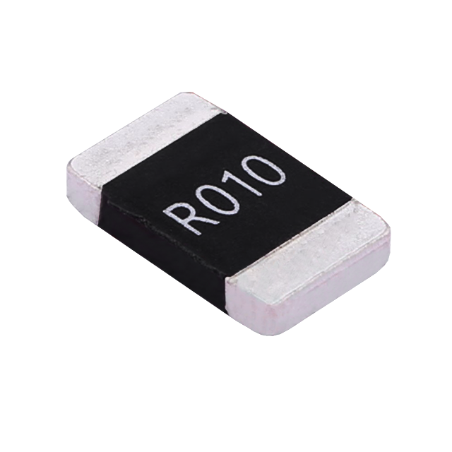
Key performance features: high power handling, ultra-low temperature drift, high overload withstand capability, low inductance at high frequency, and automotive-grade high reliability.
HoCG4527 Automotive Grade Molded Alloy Resistor
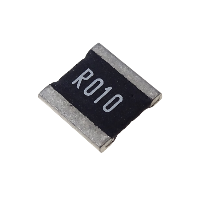
Key features: ultra-high current-carrying capability, ultra-high stability, ultra-low temperature drift, and low inductance at high frequency.
HoCG2728 Automotive Grade Molded Alloy Resistor

Alloy resistors, with their unique technical advantages—ultra-low resistance, low temperature drift, high power handling, low parasitic parameters, and strong pulse withstand capability—have become core components in current sensing, overload protection, and load matching circuits for EV charging stations.
Alloy Resistor Applications in New Energy