Layout design for parallel use of Kelvin structure resistors
author: Milliohm Electronic
2025-10-24
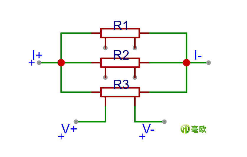
I. Core Principles: Separate Current and Voltage Paths and Maintain Symmetry
① Current Path (I+, I-): A thick, symmetrical, and uniform current path carries the main current. It should be connected via thick wire or copper. The current path lengths and impedances of the three resistors should be as consistent as possible to avoid uneven current distribution (overloading a resistor) due to differences in parasitic parameters.
② Voltage Detection Path (V+, V-): A thin, independent, and interference-free voltage path transmits only weak detection signals. It should be connected using independent, thin wires and strictly derived from the resistor's voltage terminals (V+, V-). Sharing wires with the current path is prohibited (otherwise, additional resistance will be introduced, undermining the accuracy advantage of the Kelvin structure).
As shown in Figure 1 below, when three resistors are used in parallel, the voltage detection pin of one of the resistors can be used (the voltage pins of the other two resistors are not set to electrical network signals and are left floating, with only pad connections for fixing. Because the voltage drops of all resistors in the parallel resistor network are the same, there is a common voltage between the resistors connected in parallel, and this voltage is the same for all parallel-connected components).

III. Specific Routing Steps and Details
① Resistor Layout: Symmetrical and Compact to Reduce Parasitic Parameters
Place the three Kelvin resistors side by side or in a compact triangle with even spacing. Ensure that each resistor is physically the same distance from the current sink and voltage sensing point to minimize parasitic inductance or resistance variation caused by varying wiring lengths. The resistor pins should be oriented in the same direction (e.g., current terminals facing outward, voltage terminals facing inward) to facilitate centralized routing.
② Current Path (I+, I-) Routing: Use a busbar or copper patch, with symmetrical branches as much as possible.
Busbar/Copper Area Design: Input (I+): Create a common I+ busbar (recommended copper thickness ≥ 35μm, width calculated based on total current, e.g., ≥ 5mm for a total current of 100A). Connect the I+ terminals of the three resistors to this busbar via branch wires of equal length and width (branch length difference ≤ 1mm, consistent width). Output (I-): Similarly, set up a common I- bus. Connect the I- terminals of the three resistors to this bus via branch wires of equal length and width.
Avoid current crossing: The current path must be kept away from the voltage detection path to reduce electromagnetic interference (large currents can generate magnetic fields that interfere with voltage signals).
③ Voltage Detection Path (V+, V-) Wiring: Independent leads, directly connected to the detection chip.
Independent leads: Lead the V+ terminal of one of the three resistors through a separate thin wire (e.g., 0.2mm wide with 18μm copper thickness, as the current is extremely low). The same applies to the V- terminal of each resistor.
Do not connect the V+ lead of a resistor to the I+ bus (or the I+ terminal of another resistor). It must be strictly connected to the V+ terminal of that resistor. Similarly, connect the V- lead only to its own V- terminal.
Short and straight: The voltage detection line should be as short as possible to avoid winding and reduce parasitic resistance and noise.

*** If you would like to learn more about our products or solutions, or their application in specific scenarios, please feel free to contact us for technical support.
Differences in resistance between FeCrAl and Kama alloy
Alloy resistor heat dissipation design: a hierarchical strategy from source to system
Related Article
Core Advantages: Pure Alloy Material | Electron Beam Welding Process | Fully Certified & Compliant | Precision Selection & Tailored Adaptation
Elevating Current Sensing Performance: The RS3812(3824) Series Bare Alloy Resistors
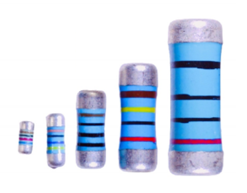
As precision power resistors, wafer resistors (commonly known as MELF resistors, an acronym for Metal Electrode Leadless Face) adopt a leadless cylindrical configuration. Their construction comprises a ceramic base substrate coated with a metallic thin film that forms the functional resistive layer.
The Underrated Powerhouse: Why Wafer Resistors Are the Unsung Heroes of High-End Electronics