The Underrated Powerhouse: Why Wafer Resistors Are the Unsung Heroes of High-End Electronics
Wafer resistors—also known as MELF resistors (Metal Electrode Leadless Face) or cylindrical metal film resistors—are precision power resistors engineered with a leadless cylindrical architecture, a ceramic substrate, and a metallic thin-film resistive layer. What sets them apart is their unique ability to reconcile two previously conflicting demands: the compact footprint and automated assembly compatibility of chip resistors, and the thermal stability and power robustness of through-hole types. With exceptional precision, low TCR, minimal noise, high-voltage endurance, and ultra-low parasitic inductance, they are the go-to choice for telecommunications, medical instrumentation, precision measurement, automotive systems, and industrial automation—applications where circuit fidelity and long-term reliability are non-negotiable. In short, they are a cornerstone component in today's high-end electronic infrastructure.
Compared with conventional carbon film or thick-film chip alternatives, wafer resistors are fabricated using semiconductor-grade processes such as vacuum deposition and photolithographic etching. This enables tolerances down to ±0.05% and TCR values from ±5 ppm/°C to ±50 ppm/°C. Meanwhile, the leadless design drastically curbs parasitic inductance at high frequencies—a persistent challenge in through-hole designs—while delivering superior current and voltage handling beyond the reach of standard chip resistors. The result: superior electrical performance and long-term dependability in the most demanding circuit environments.
I. Core Structure & Working Principle
(1) Core Structure
Designed for precision and reliability, the wafer resistor consists of six key components working together to optimize electrical performance and mechanical strength. the structure is as follows ( From inside to out ) :
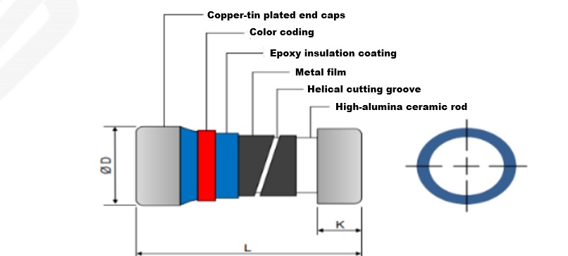
① Ceramic Substrate – The Foundation: The ceramic substrate is the backbone of the wafer resistor. Made from high-performance materials like alumina, this cylindrical core offers exceptional insulation, thermal conductivity, and heat resistance. It not only supports the resistive layer but also efficiently channels heat away from the component. Its material quality and size directly influence the resistor's power rating and thermal performance—making it a cornerstone of long-term reliability.
② Resistive Layer – The Heart of Precision: The resistive layer is an ultra-thin metal film deposited onto the ceramic substrate using advanced PVD techniques such as vacuum evaporation or sputtering. Materials like nickel-chromium, platinum, or tungsten are selected for their high-temperature stability. Through precise photolithography and etching, the layer's dimensions are controlled down to microscopic levels, determining the exact resistance value. This is the primary reason wafer resistors achieve precision far beyond standard resistors. In premium models, laser trimming further refines the value to meet the tightest tolerances.
③ End Electrodes – Reliable Connections: The end electrodes are applied to both ends of the ceramic substrate using highly conductive metals like copper or silver. They bridge the resistive layer to the external circuit. A tin or gold plating is added to ensure excellent solderability and corrosion resistance, guaranteeing a stable, low-resistance connection to PCBs or wires. For high-power applications, enlarged electrodes are used to handle greater currents.
④ Insulation Coating – Built to Last: A durable coating of epoxy resin or ceramic encapsulates the resistive layer and electrodes. This protective layer shields the internal components from dust, moisture, and chemicals, prevents oxidation, and reinforces electrical insulation—all of which extend the product's service life and reliability in demanding environments.
⑤ Trimming Line – Fine-Tuning Accuracy: On high-precision models, a trimming line is laser-etched onto the resistive layer. By adjusting its length and width, the resistance can be calibrated to exact specifications. This process is critical to achieving the ±0.05% tolerances that make wafer resistors the preferred choice for precision-critical applications.
⑥ Marking – Clear Identification: Printed on the insulation coating, the marking provides essential details at a glance: nominal resistance, tolerance, power rating, and temperature coefficient. Some products also feature manufacturer codes for traceability. Resistance values are displayed using a four-digit system where "R" stands for the decimal point—so R050 means 0.05Ω, and 1001 means 1KΩ.
(2 ) Operating Principle
The fundamental operating principle of wafer resistors aligns with that of standard resistors, rooted in Ohm's law and the Joule heating effect. As current traverses the resistive layer, free electrons in the metallic film undergo collisions with lattice atoms, converting electrical energy into heat and thereby performing critical circuit functions including current limiting, voltage division, power loading, and signal conditioning.
What distinguishes wafer resistors from their conventional counterparts is their structural superiority, which translates into enhanced performance:
① The leadless construction dramatically curtails parasitic inductance and parasitic capacitance, mitigating the risks of circuit oscillation and signal degradation at high frequencies, thus rendering wafer resistors ideally suited for high-frequency circuit designs.
② The exceptional thermal conductivity of the ceramic substrate, in conjunction with the insulation coating, facilitates efficient heat evacuation, enabling the component to sustain higher power dissipation while preserving thermal stability over extended operational periods.
③ The resistive layer, fabricated through precision deposition and photolithographic etching, guarantees tight resistance tolerances with negligible drift attributable to temperature fluctuations or long-term aging. This translates into a low temperature coefficient of resistance and minimal noise, ensuring consistent and reliable performance in demanding environmental conditions.
II. Manufacturing Process of Wafer Resistors
The manufacturing process of wafer resistors represents a sophisticated integration of semiconductor fabrication methodologies and conventional resistor production techniques. Characterized by stringent process controls and meticulous quality assurance, the core production sequence comprises five critical stages, each of which exerts a direct influence on the performance and precision of the finished component. The process is detailed as follows:
(1) Substrate Preprocessing: High-purity ceramic materials are selected and processed into cylindrical substrates via pressing and sintering operations. The substrate surfaces are subsequently subjected to grinding, cleaning, and drying treatments to eliminate surface contaminants and irregularities, thereby ensuring a smooth and pristine surface finish. This preparatory step is fundamental to subsequent resistive layer deposition and critically determines the interfacial adhesion strength between the resistive layer and the ceramic substrate.
(2) Resistive Layer Deposition: Employing vacuum evaporation or sputtering techniques, metallic or alloy materials are heated to vaporization within a controlled vacuum environment, enabling the metal vapor to condense uniformly onto the ceramic substrate surface, thereby forming an ultra-thin, homogeneous metal film—the resistive layer. By meticulously regulating parameters such as evaporation temperature, deposition duration, and vacuum pressure, the thickness of the resistive layer is precisely controlled, which in turn establishes the preliminary resistance value range.
(3) Photolithography and Etching: A photoresist layer is applied onto the resistive layer surface, and the designed resistor pattern is transferred onto the photoresist through photolithographic processing. The superfluous resistive material is then removed via etching to yield the desired resistor geometry (e.g., a helical configuration), enabling further refinement of resistor length and width for accurate nominal resistance control. For high-precision variants, laser trimming is additionally implemented to create trimming lines for secondary resistance calibration.
(4) End Electrode Fabrication: Through evaporation or electroplating processes, highly conductive metals are deposited at both extremities of the ceramic substrate to form the end electrodes. These electrode surfaces are subsequently plated with tin or gold to optimize solderability and oxidation resistance, ensuring robust electrical contact with the resistive layer and stable conductive performance.
(5) Encapsulation and Testing: An insulation coating is applied to the resistor body and cured to finalize product encapsulation. The finished components undergo comprehensive testing encompassing resistance tolerance, temperature coefficient of resistance (TCR), power dissipation capability, insulation integrity, and solder heat resistance, among other parameters. Conforming products are approved for shipment, while non-conforming units are rejected, guaranteeing consistent quality and reliability of all delivered products.
III. Main Classifications and Characteristics of Wafer Resistors
Wafer resistors are available in a variety of types, differentiated by precision, power rating, package dimensions, and intended application. Each category offers distinct performance attributes and application suitability to accommodate diverse circuit design requirements. The four most prevalent classification schemes and their corresponding product characteristics are presented below:
(I) Classification by Precision Grade
① Standard Precision Wafer Resistors: These devices offer precision within ±1% to ±5%, a TCR ranging from ±50 ppm/°C to ±100 ppm/°C, resistance values from 0.1Ω to 10MΩ, and power ratings from 1/8W to 1W. They are economically priced and predominantly utilized in general high-end electronic equipment where extreme precision is not critical, including consumer electronics and standard communication devices.
② High-Precision Wafer Resistors: These components provide precision from ±0.05% to ±0.5%, with a TCR of ±5 ppm/°C to ±25 ppm/°C. Manufactured using advanced deposition and photolithographic etching techniques, they offer exceptional resistance stability. Rated at 1/4W to 1W, they are specifically designed for demanding applications requiring the utmost accuracy and long-term stability, such as precision instrumentation, medical equipment, and aerospace systems.
(2) Classification by Power Rating
① Low-Power Wafer Resistors: With power ratings from 1/8W to 1/4W, these compact resistors are typically offered in 0102 and 0204 package sizes. They are tailored for miniaturized, low-power-consumption devices including smartphones, tablets, and compact sensors, performing essential circuit functions such as current limiting, voltage division, and signal conditioning.
② Medium-Power Wafer Resistors: Covering a power range of 1/4W to 1W, these devices are predominantly supplied in the 0207 package, offering an optimal balance between footprint and performance. They find extensive application in communication systems, industrial control units, and automotive electronics, where they reliably withstand moderate load transients while maintaining commendable precision and stability.
③ High-Power Wafer Resistors: Rated above 1W and featuring larger package sizes (e.g., 0309), certain variants incorporate heat-dissipation provisions. Characterized by superior current-carrying capacity and exceptional high-voltage tolerance, these resistors are deployed in high-power supply modules, variable frequency drives, and railway rolling stock equipment, where they serve to absorb surplus electrical energy and buffer current surges.
(3) Classification by Package Size
Wafer resistor package dimensions conform to standardized coding conventions, with the four most common sizes being 0102, 0204, 0207, and 0309. Each package size corresponds to specific physical dimensions and power ratings, as detailed below:
① 0102 Package: Dimensions approximately 2.00±0.10mm (length) × 1.30±0.05mm (diameter), rated at 1/8W. This represents the most compact package, ideally suited for ultra-high-density and miniaturized circuit configurations.
② 0204 Package: Dimensions approximately 3.50±0.20mm (length) × 1.40±0.15mm (diameter), rated at 1/4W. This is the most widely adopted package format, suitable for the vast majority of high-end electronic equipment.
③ 0207 Package: Dimensions approximately 5.90±0.20mm (length) × 2.20±0.20mm (diameter), rated from 1/2W to 1W. This size delivers a favorable compromise between compactness and power-handling capability.
④ 0309 Package: Dimensions approximately 9.0mm (length) × 3.0mm (diameter), rated above 1W. This larger package is specifically intended for high-power applications.
(4) Classification by Application
① Precision-Type Wafer Resistors: Engineered with a primary emphasis on high accuracy and minimal temperature drift, these resistors are predominantly employed in precision measurement instruments, medical diagnostic equipment, and ADC/DAC reference circuits, where they deliver precise resistance values critical for measurement accuracy and signal conversion fidelity.
② Power-Type Wafer Resistors: Designed with a focus on high power dissipation and high voltage endurance, these resistors are widely utilized in power supply modules, frequency converters, and braking circuits, where they perform load management, current limiting, and energy absorption functions, with the resilience to withstand instantaneous high-power surges.
③ High-Frequency-Type Wafer Resistors: Optimized for low parasitic inductance and minimal noise, these resistors are primarily deployed in RF circuits and high-frequency communication systems, where they effectively suppress high-frequency signal interference and ensure stable signal integrity.
IV. Critical Technical Specifications of Wafer Resistors
In the process of selecting and deploying wafer resistors, particular attention should be paid to the following essential technical parameters to guarantee compatibility with circuit design objectives and to mitigate the risk of component failure or system malfunction attributable to parameter discrepancies. The six most significant parameters are presented as follows:
(I) Nominal Resistance and Precision
Nominal resistance constitutes the fundamental parameter of wafer resistors, expressed in ohms (Ω), with a typical range extending from 0.1Ω to 22MΩ, thereby covering low-, medium-, and high-resistance intervals to accommodate diverse circuit functions including current limitation, voltage division, and load management. Precision (resistance tolerance) defines the permissible deviation between the actual resistance value and the nominal specification. Standard tolerance grades include ±0.05%, ±0.1%, ±0.25%, ±0.5%, ±1%, and ±5%. Higher precision grades yield superior resistance stability albeit at increased cost. Precision-critical applications warrant the selection of ±0.05% to ±0.5% tolerance products, whereas ±1% to ±5% tolerance variants suffice for general high-end applications.
Wafer resistors employ a four-digit coding convention for resistance value notation, wherein "R" serves as the decimal point designator. For instance, 0100 corresponds to 10Ω, 1001 to 1KΩ, 1004 to 1MΩ, and R050 to 0.05Ω. Zero-ohm resistors are denoted as R0R0, rather than R000.
(2) Rated Power
Rated power denotes the maximum continuous power dissipation that a wafer resistor can sustain under specified ambient temperature conditions (typically 25°C), quantified in watts (W). Standard power ratings include 1/8W, 1/4W, 1/2W, 1W, and higher. Exceeding the rated power threshold can induce thermal overstress, resistance drift, insulation coating degradation, or catastrophic failure. During component selection, it is prudent to incorporate a power derating margin of no less than 30% above the actual circuit power consumption. For pulsed operation scenarios, peak power withstand capability warrants particular scrutiny to ensure tolerance of transient high-power excursions.
(3) Temperature Coefficient of Resistance (TCR)
The temperature coefficient of resistance quantifies the rate of resistance change per 1°C variation in ambient temperature, expressed in ppm/°C (parts per million per degree Celsius). Lower TCR values denote superior temperature stability. Wafer resistors offer TCR ratings spanning ±5 ppm/°C to ±100 ppm/°C. High-precision devices can achieve TCR as low as ±5 ppm/°C, whereas standard-grade products typically exhibit ±50 ppm/°C to ±100 ppm/°C. In high-temperature operating environments—such as automotive engine compartments or industrial furnace installations—low-TCR products are strongly recommended to mitigate temperature-induced resistance drift that could compromise circuit accuracy.
(4) Operating Temperature Range
This parameter defines the temperature interval over which the wafer resistor can reliably function, typically ranging from -55°C to +150°C, with certain high-temperature variants rated up to +175°C. Operation beyond the upper temperature limit can precipitate performance degradation and accelerated aging, while operation below the lower limit may impair electrical conductivity. Consequently, product selection should be guided by the ambient temperature profile of the intended application.
(5) Withstanding Voltage and Insulation Resistance
Withstanding voltage (dielectric withstand voltage) refers to the maximum voltage that may be applied across the resistor terminations, typically ranging from 200V to 700V. Products with higher power ratings and larger physical dimensions offer enhanced withstand voltage capabilities. In high-voltage applications, it is imperative to select devices with adequate voltage ratings to preclude dielectric breakdown. Insulation resistance, which characterizes the insulation integrity between the resistor body and its terminations, is generally specified at ≥100MΩ (at 25°C, 500V DC). Insufficient insulation resistance can precipitate current leakage, giving rise to potential safety concerns.
(6) Package Size and Packaging Method
Package size selection should be informed by PCB layout constraints and available mounting space. The four standard package sizes—0102, 0204, 0207, and 0309—feature precise, standardized dimensions that are fully compatible with automated pick-and-place assembly processes. Packaging configurations comprise tape-and-reel packaging and bulk packaging. Tape-and-reel packaging is optimized for high-volume automated production, with standard quantities of 2,000 pieces per reel or 3,000 pieces per reel, whereas bulk packaging is more suitable for small-batch prototyping or manual soldering operations.
V. Application Scenarios of Wafer Resistors
By virtue of their inherent advantages—including high precision, low temperature coefficient of resistance, low noise, high voltage endurance, and minimal parasitic inductance—wafer resistors are predominantly employed in high-end applications where circuit accuracy and stability are of paramount importance. Their deployment spans a diverse range of industries, encompassing telecommunications, healthcare, industrial automation, automotive, and aerospace sectors. The specific application scenarios are elaborated below:
(I) Telecommunications Equipment
This sector constitutes one of the primary application domains for wafer resistors, covering routers, switches, base station equipment, optical transceiver modules, and related devices. Within telecommunications circuits, wafer resistors perform signal conditioning, current limiting, and voltage division functions. Their low-noise characteristics and low parasitic inductance contribute to stable high-frequency signal transmission, mitigate signal distortion, and enhance both transmission efficiency and operational stability of communication systems. In optical modules, high-precision wafer resistors are employed for optical signal intensity calibration, thereby ensuring data transmission integrity.
(2) Medical Devices
Wafer resistors are ideally suited for precision medical instrumentation, including diagnostic equipment, patient monitoring systems, and blood glucose analyzers. These devices impose exceptionally rigorous demands on circuit accuracy and long-term stability. Leveraging their high precision and low TCR, wafer resistors deliver accurate resistance values essential for signal detection and data acquisition, thereby guaranteeing measurement fidelity. For example, in patient monitors, they contribute to the stable acquisition and transmission of physiological signals such as heart rate and blood pressure, reinforcing the reliability of clinical diagnostics.
(3) Industrial Control
Wafer resistors find extensive application in industrial automation control systems, servo drives, frequency converters, and precision sensors. In servo motor control circuits, they are utilized for current sensing and current limiting to facilitate precise and responsive motor regulation. In braking circuits of frequency converters, power-type wafer resistors absorb regenerative energy generated during motor deceleration, preventing voltage surges that could compromise equipment integrity. In precision sensors, high-accuracy wafer resistors perform signal calibration functions to elevate detection precision.
(4) Automotive Electronics
Wafer resistors are well-adapted to automotive electronic systems, including on-board electronic control units (ECUs), autonomous driving systems, instrument panels, and in-vehicle power management modules. The automotive environment is characterized by wide temperature variations and severe mechanical vibration. Wafer resistors, distinguished by their high-temperature tolerance, vibration resistance, and robust stability, are capable of reliable long-term operation under such harsh conditions. They perform current limiting, voltage division, and signal conditioning functions to sustain stable performance of automotive electronic systems. In autonomous driving applications, for instance, they stabilize sensor signals, thereby contributing to vehicle operational safety.
(5) Precision Instrumentation and Aerospace
Wafer resistors are deployed in precision measurement instruments, oscilloscopes, and aerospace systems—applications that demand the highest standards of precision, stability, and reliability. In precision measurement instruments, wafer resistors function as standard loads or reference resistors to ensure measurement accuracy. In aerospace equipment, their resistance to extreme temperature excursions, radiation tolerance, and exceptional stability render them suitable for space and high-altitude environments, ensuring dependable equipment performance under the most demanding conditions.
(6) Consumer Electronics
Wafer resistors are primarily utilized in high-end consumer electronic devices, including smartphones, tablets, laptops, and premium household appliances, where they fulfill power management and signal conditioning roles. Their compact footprint and high precision align with the industry trends toward miniaturization and high-density circuit layouts in consumer electronics, while simultaneously enhancing product reliability and operational lifespan.
VI. Selection Criteria and Operational Precautions for Wafer Resistors
(I) Selection Criteria
① Align Precision and Temperature Coefficient with Application Requirements: Select the appropriate precision grade in accordance with circuit accuracy specifications. For applications demanding high precision, priority should be given to products offering ±0.05% to ±0.5% tolerance and ±5 ppm/°C to ±25 ppm/°C TCR. For general high-end applications, products with ±1% to ±5% tolerance and ±50 ppm/°C to ±100 ppm/°C TCR provide a cost-effective solution that balances performance and economy.
② Determine Appropriate Power Rating and Withstanding Voltage: Based on actual circuit power consumption, select a product with a suitable power rating while incorporating a minimum derating margin of 30%. Additionally, taking into account the circuit's operating voltage, choose a product with adequate withstand voltage capability to preclude dielectric breakdown.
③ Select Compatible Package Size: Package size should be determined based on PCB layout constraints and available installation space. The 0102 and 0204 packages are optimal for compact, high-density layouts, whereas the 0207 and 0309 packages are more appropriate for medium- to high-power applications, ensuring convenient assembly without compromising other components.
④ Account for Operating Environment: For applications subjected to high temperatures and mechanical vibration—such as automotive electronics and industrial equipment—select models specifically designed with high-temperature endurance and vibration resistance. In high-frequency applications, products featuring low parasitic inductance and low noise should be chosen to maintain stable circuit performance.
(2) Operational Precautions
① Do Not Exceed Power or Voltage Ratings: Adhere strictly to the rated specifications during operation. Operation beyond the rated power can induce thermal stress, resistance drift, and degradation of the insulation coating, while exceeding the voltage rating may result in dielectric breakdown and associated safety risks. For pulsed operation, verify peak power ratings to avoid transient overload-induced failure.
② Observe Proper Soldering Practices: During soldering, the soldering temperature should be maintained below 350°C and the soldering duration should not exceed 3 seconds to prevent end electrode detachment or resistive layer damage attributable to prolonged high-temperature exposure. The soldering point should be positioned away from the resistor body to minimize thermal conduction effects on resistor performance.
③ Plan Layout and Heat Dissipation Strategically: High-power wafer resistors generate significant heat during normal operation. PCB layout should be carefully planned to provide sufficient clearance for heat dissipation and to avoid close placement adjacent to heat-sensitive components such as capacitors and integrated circuits. Where necessary, heatsinks may be incorporated to improve thermal management and extend product service life.
④ Protect Against Environmental Contaminants: Avoid installing wafer resistors in environments with excessive dust, moisture, or oil contamination, which can penetrate the internal structure and degrade resistor performance. In harsh environments, sealed protective enclosures should be considered.
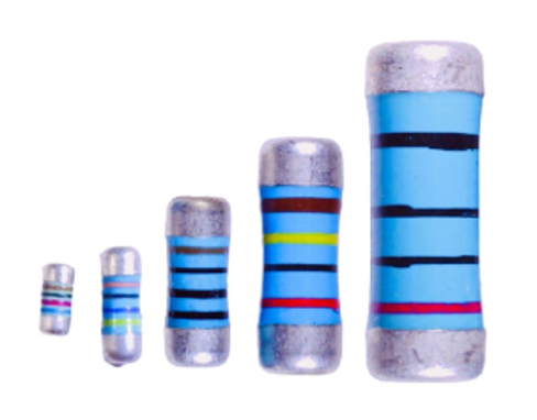
⑤ Differentiation and Identification: When wafer resistors are intermixed with thick-film chip carbon film resistors, they can be distinguished through three approaches: Visual inspection—wafer resistors typically exhibit a blue body with four color bands, whereas carbon film resistors generally feature a tan/yellowish body with three color bands. Temperature-based testing—apply a heated soldering iron in proximity; the resistor exhibiting minimal resistance change is the wafer resistor. Film layer examination—scrape away the protective coating; a bright white metallic film signifies a wafer resistor, while a black film indicates a carbon film resistor.
VII. Comparison Between Wafer Resistors and Conventional Resistor Types
To provide a clearer perspective on the distinct advantages of wafer resistors, the key differentiators between wafer resistors and conventional carbon film resistors, as well as thick-film chip resistors, are summarized below for ease of reference during the selection process:
(1) Versus Carbon Film Resistors: Wafer resistors deliver substantially higher precision (achieving tolerances as low as ±0.05% compared to ±5%~±10% for carbon film types), exhibit significantly lower temperature coefficients (±5 ppm/°C~±100 ppm/°C vs. ±100 ppm/°C~±500 ppm/°C), benefit from reduced parasitic inductance attributable to their leadless architecture, and demonstrate superior high-voltage and high-current capability along with lower noise characteristics. However, these performance advantages come at a higher cost, positioning wafer resistors as the preferred choice for high-end applications, while carbon film resistors remain more suitable for cost-sensitive, general-purpose scenarios.
(2) Versus Thick-Film Chip Resistors: Wafer resistors offer enhanced long-term stability, reduced temperature drift, superior high-voltage and high-current performance, and lower parasitic inductance, rendering them particularly well-suited for high-frequency and precision-critical applications. Thick-film chip resistors, in contrast, provide a more compact footprint and lower unit cost, making them the go-to option for mainstream consumer electronics where board space is at a premium, albeit with comparatively lower precision and stability than their wafer resistor counterparts.
VIII. Conclusion
Wafer resistors represent a class of high-precision, high-stability power resistors that, through their leadless cylindrical architecture and sophisticated manufacturing processes, successfully synergize the advantages of both surface-mount chip resistors and through-hole resistors. They fulfill an indispensable role in high-end applications characterized by demanding precision, high-frequency operation, elevated voltages, and harsh environmental conditions. Their fundamental value proposition resides in the provision of accurate and stable resistance values, effectively mitigating the adverse effects of temperature variations and environmental factors on circuit performance, and thereby underpinning the reliable operation of advanced electronic systems.
As the telecommunications, healthcare, automotive electronics, and aerospace industries continue their rapid advancement, the performance expectations for electronic components in terms of precision, stability, and reliability are steadily escalating. Consequently, the application landscape for wafer resistors is poised for continued expansion, while the technology itself will evolve toward ever-higher precision, more compact packaging, increased power-handling capacity, and lower temperature coefficients, progressively addressing the requirements of an expanding array of high-end applications. When selecting and deploying wafer resistors, careful consideration must be given to circuit-specific requirements and operating environments, with due attention to the critical parameters and adherence to the selection guidelines and operational precautions detailed herein, to fully realize their performance potential and ensure dependable system operation.
Elevating Current Sensing Performance: The RS3812(3824) Series Bare Alloy Resistors
Optimization strategy for current transmission and thermal management
Related Article