Anti-detachment technology for the soldering of alloy resistors and bus bars
I: Main Functions and Operation Steps of SMD Red Adhesive
The main functions of SMD Red Adhesive include: physical fixation to prevent components from detaching or shifting during the reflow soldering process; auxiliary positioning to ensure components maintain correct positions during soldering; high-temperature resistance — the SMD Red Adhesive cures at around 180°C and can withstand subsequent high-temperature soldering processes; and good compatibility, with no negative impact on soldering quality.
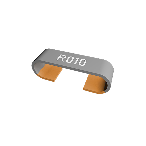
As shown in the figure below, the soldering of bottom-layer SMD alloy resistors and bus bars interferes with the top-layer through-hole components. If the SMD components are mounted first and then subjected to wave soldering, the resistors and bus bars will fall off. If wave soldering is performed first followed by SMD mounting, the reflow soldering process cannot be applied. The solution is to first use SMD Red Adhesive to fix the alloy resistors and bus bars, then perform reflow soldering, and finally conduct wave soldering for the through-hole components.

The operation steps are as follows: first, dispense SMD Red Adhesive onto the PCB; then place the components onto the adhesive and ensure accurate positioning; next, perform the first reflow soldering, during which the SMD Red Adhesive cures under high temperature, firmly fixing the components onto the PCB; finally, turn the PCB over and perform the second reflow soldering.
In the mixed process of SMT and DIP, to avoid the double reflow situation of one reflow soldering for single-sided mounting followed by one wave soldering, SMD Red Adhesive can be dispensed at the center of chip components and devices on the wave soldering side of the PCB. This allows solder to be applied in a single pass during wave soldering, eliminating the need for the solder paste printing process.
II. Application of Solder Alloys with Different Melting Points
Employing solder alloys with different melting points is another effective approach to address the issue of secondary soldering.
The underlying principle is to use a high-melting-point solder alloy during the first reflow soldering process and a low-melting-point solder alloy during the second reflow soldering process, thereby minimizing thermal impact on the first solder joints.Typical application strategies are illustrated below. As shown in the figure:

During the first reflow soldering process for mounting SMD capacitors on a PCB, a high-melting-point solder such as Sn-Ag-Bi ternary alloy or other high-melting-point alloys is used. Subsequently, during the wave soldering process for attaching the shunt, a low-melting-point solder such as Sn42Bi58 (melting point 138°C) is applied, thereby creating a melting point gradient. Precise control of the soldering temperature ensures that the second soldering process does not cause remelting of the first solder joints.
A practical example is as follows: some manufacturers first attach the circuit board to a copper heat-spreading base using a high-melting-point solder, and then mount the LED onto both the copper base and the circuit board using a low-melting-point solder. Since the low-melting-point solder has a lower melting point, it does not remelt the previously applied high-melting-point solder during subsequent soldering, thereby effectively addressing the secondary soldering challenge.
It is worth noting that the selection of low-melting-point solders may be constrained by the operating temperature range of the final product, while high-melting-point alloys often necessitate higher reflow temperatures, which may pose a risk of thermal damage to both components and the PCB.
III. Reflow Soldering Temperature Profile Optimization
Optimizing the reflow soldering temperature profile is a key technical approach to preventing component detachment during secondary soldering. By configuring the oven’s temperature settings—specifically, keeping the molten zone temperature of the lower heating zone slightly lower than that of the upper heating zone—thermal shock to previously soldered components can be significantly reduced.
Key strategies for temperature profile optimization include:
-
Preheat zone: Apply a stepped ramp‑up strategy with a ramp rate of 1.5–2°C/s to avoid thermal shock and minimize solder paste spattering.
-
Soak (activation) zone: Maintain a temperature range of 150–180°C to fully activate the flux in the solder paste and remove oxides.
-
Reflow zone: Set the peak temperature precisely according to the solder type. For high‑temperature solder paste (melting point 217°C), the recommended peak temperature is 245±5°C; for low‑temperature solder paste (melting point 138°C), it is 180±5°C.
For double‑side reflow soldering, special attention must be paid to temperature control. On the first reflow (bottom side), use a high‑temperature solder paste such as SAC305 (melting point 217–221°C) with a peak temperature of 245–260°C to ensure the formation of a stable intermetallic compound (IMC) layer on the bottom‑side solder joints. On the second reflow (top side), the peak temperature should be at least 30°C lower than that of the first reflow (e.g., 165–185°C) to avoid remelting the bottom‑side solder.
Another practical technique is to blow cold air from beneath the oven, which lowers the temperature on the bottom side of the PCB and keeps it below the solder melting point during the second reflow. However, this approach requires careful management of the temperature difference between the top and bottom sides to prevent excessive internal stress.
Application Analysis and Selection Guide for Alloy Resistors in Precision Equipment
Suppression and Optimization of EMF in Shunt Resistors
Related Article